
Silicon epitaxy under ultra-high vacuum (UHV) is a challenging process required not only for Si technology, but also for III-Vs integration on Si. An in situ compatible Si buffer layer is desirable before the growth of a III-V buffer layer, usually GaP, without intermediate air-exposure. The extremely high temperatures required for Si Knudsen cells, even to obtain moderate growth rates, may cause contamination or doping from cell surroundings. Electron beam assisted evaporation or direct Si filament heating are usually the main alternatives for solid-source molecular beam epitaxy (MBE). Gaseous precursors are used in chemical beam epitaxy (CBE) systems, but carbon-containing precursors can promote SiC nucleation and growth inhibition. Among gaseous precursors, silane is widely used, although it is highly hazardous. Higher-order silanes (SinH2n+2) offer a promising alternative due to their lower vapor pressures: trisilane (n=3) is liquid at room temperature with subatmospheric vapor pressure (about 300 mbar) allowing its injection on MBE or CBE chambers without the need of a carrier gas such as H2.
In this work we present preliminary results on the growth of Si on nominally oriented Si (001) substrates, using Si3H8 in a CBE system. During growth, the system pressure -with a 2800 l/s turbo pump with cryopanel assistance- was in the range 1×10⁻⁹ to 1×10⁻⁷ mbar, depending on the gas flux.
As-received Si wafers were dipped in diluted HF to remove the native oxide layer. Si substrate temperature was increased under UHV up to 750 ºC to desorb H and some possible SiO traces, until a (2×2) like surface reconstruction was observed by reflection high-energy electron diffraction (RHEED), due to the superposition of (1×2) and (2×1) domains on adjacent Si(001) terraces.
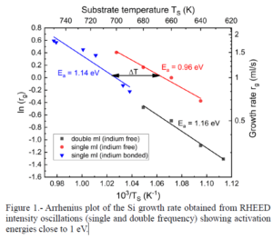
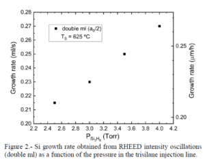
Si growth with Si3H8 can take place at moderate temperatures, in the range between 580 and 700 ºC, allowing thermal decomposition of precursor molecules on the substrate surface, without needing a high-temperature cell for precursor pre-cracking. Growth rates were measured using RHEED intensity oscillations, observing single- and double-frequency harmonics corresponding to the growth of double (a0/2) and single monolayers (a0/4), respectively. The growth rate increases with the substrate temperature due to the thermal activation of the precursor and/or H desorption on the surface, with an activation energy close to 1 eV, as shown in fig. 1. A slight shift is observed in the curves (ΔT ≈30 ºC) when using indium free or indium bonding sample holders, likely due to some inaccuracy on the pyrometer readings. Additionally, the growth rate was proportional to the pressure of the gas injection line (fig. 2), allowing tight control of the growth process. Auger spectra of Si samples after growth do not show traces of any contaminant, up to the resolution limit of the technique.
This growth method, developed in a CBE system, can be readily adapted to MBE systems by adding both, a single gas injector with flux control, and a suitable pumping system.
The incorporation of N into GaP induces an indirect-to-direct band gap transition, as described by the band anticrossing model [1]. Furthermore GaP1-xNx is lattice matched to Si for x = 0.021, with a bandgap energy close to 1.95 eV at 300 K, which makes it an ideal candidate to integrate light-emitting devices and photovoltaic cells with the standard Si technology. In this work, we report a comprehensive study on the chemical beam epitaxy (CBE) of GaP1-xNx thin films on (001)-oriented GaP-on-Si substrates. Specifically, we systematically investigate the impact of the growth parameters on the incorporation of N, the structural quality, and the morphological properties using a wide variety of experimental techniques including reflection high-energy electron diffraction (RHEED), high-resolution x-ray diffraction (HRXRD), combined ion beam techniques (RBS and NRA), transmission electron microscopy (TEM) and atomic force microscopy (AFM).
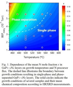
The analysis of the chemical composition by HRXRD, RBS and NRA as a function of the growth parameters revealed that the mean N content increases linearly with the flux of the N precursor and decreases exponentially with the growth temperature according to an Arrhenius’ law, with an activation energy of 0.83 eV [2]. Our study also evidences the existence of two different growth regimes: a single-phase regime characterized by a well-defined chemical composition, and a phase-separated growth regime characterized by the presence of two chemical phases with different N content.
The monitoring of the growing surface in situ by RHEED and ex situ by AFM demonstrated that single-phase samples exhibit a smooth surface morphology, while phase separated ones exhibit a corrugated surface due to the formation of 3 dimensional (3D) islands elongated along the [110] direction. The additional analysis of the temporal evolution of the RHEED intensity indicates all samples grow layer-by-layer during the early growth stages, regardless of the final growth regime. However, for the phase-separated samples, the layer-by-layer growth mode is only maintained up to reaching a certain critical thickness. Then, there is the 2D-3D growth mode transition. All these results are illustrated in the growth diagram shown in Figure 1, that depicts how the mean chemical composition and the boundary between the two different growth regimes depend on the growth parameters [2].
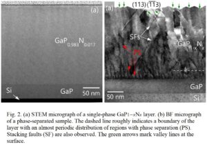
To study the material quality on atomic scale as well as to unveil the origin of the two different chemical phases, the samples were investigated by TEM. This study showed that single-phase samples have a high structural perfection and a uniform chemical composition (Fig. 3a). In contrast, phase-separated samples show abundant extended defects and a highly inhomogeneous N distribution (Fig. 3b). In particular, the N content is higher near the interface with the GaP buffer layer and exhibit strong lateral compositional modulations perpendicular to the [110] direction, most likely related to the 2D-3D transition observed by RHEED.
References
[1] W. Shan, W. Walukiewicz, K. M. Yu, J. Wu, J. W. Ager III, E. E. Haller, H. P. Xin, C. W. Tu, Appl. Phys. Lett. 76, 3251 (2000).
[2] K. Ben Saddik, B. J. García, S. Fernández-Garrido, APL Mater. 9, 121101 (2021).
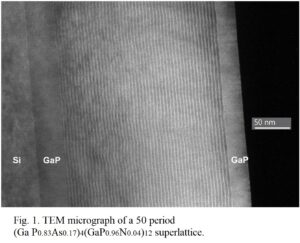
The quaternary dilute-nitride compounds GaP1-x-yAsxNx and Ga1-yInyP1-xNx are some of the very few III-V materials that can be grown lattice-matched to Si with the ideal band gaps for the fabrication of double- and triple-junction tandem solar cells in combination with a bottom Si solar cell, promising maximum photoconversion efficiencies of 43 and 47%, respectively. These materials, known since the late nineties, are however extremely challenging to fabricate with the compositional control and structural quality demanded in photovoltaics. On the one hand, as quaternary compounds, they contain 2 or 3 different group-V elements, which complicates the control of the alloy composition and system design and maintenance. On the other hand, as these materials are highly mismatched alloys, since N has a large difference on electron affinity and atomic radius when compared with As o P, they are susceptible to chemical phase separation during growth [1]. In this work, we explore the possibility of growing the quaternary compound GaP1-x-yAsyNx on Si, not in the form of a thick layer [2], as attempted so far, but as a strain-balanced short-period superlattice (SPSL) made from the two simpler ternary compounds, namely, GaAsyP1-y and GaP1-xNx[3].
All samples were fabricated by chemical beam epitaxy (CBE) on commercial GaP-on-Si(001) nominally oriented template substrates, free of antiphase domains, with an atomically smooth surface. Prior to the growth of GaPAsN based SPSLs, we analyzed the epitaxy and properties of GaP1-yAsy and GaP1-xNx compounds. Chemically homogeneous GaP1-yAsy layers were grown with 0.09 ≤ y ≤ 0.36 by varying the ratio between the As and P gas precursors. The epitaxy of GaP1-xNx alloys was probed to be far more challenging. Up to x = 0.04, it is possible to grow in a layer-by-layer fashion single-phase films with smooth surfaces and homogeneous luminescence properties characterized by carrier localization phenomena, a band gap energy well described by the band anti-crossing model. Nevertheless, for x > 0.04, the layers become thermodynamically unstable against the formation of lateral compositional and morphological fluctuations along the [110] direction upon exceeding a critical thickness of about 5 nm. These results establish the main constraints for the synthesis of GaP1-x-yAsyNx SPSLs by CBE.
For the fabrication of these type II SPSLs, we previously used both the Kronig-Penney model and the transfer matrix method to estimate the ranges of layer thicknesses and chemical compositions to obtain strain-balanced SPSLs on Si with delocalized electronic states, as desired to facilitate the extraction of photogenerated carriers in photovoltaics. Samples were characterized by several techniques, such as reflection high-energy electron diffraction (RHEED), high-resolution x-ray diffraction (HRXRD), transmission electron microscopy (TEM), spectroscopic ellipsometry (SE) and photoluminescence.
The results obtained so far demonstrate the possibility of fabricating both GaP/GaP1-xNx and GaP1-yAsy/GaP1-xNx SPSLs with a mean lattice parameter close to Si and bandgap energies of about 1.98 and 1.81 eV at 12 K by using a superlattice period of 16 monolayers with x values of 0.03 and 0.04 respectively, as shown in the TEM micrograph of figure 1.
References
[1] K. Ben Saddik, B. J. García, S. Fernández-Garrido, APL Mater. 9, 121101 (2021).
[2] K. Ben Saddik, A. F. Braña, N. López, W. Walukiewicz, B. J. García, J. Appl. Phys. 126, 105704 (2019).
[3] K. Kharel and A. Freundlich, J. Appl. Phys. 124, 095104 (2018).